The Complexities of High-Power Optical Coatings
In today's optics industry, many precision optical elements receive coatings in order to improve their transmission or reflection for certain wavelengths or polarization states. The most common types of coatings are anti-reflection (AR), high-reflective (mirror), beamsplitter, and filter. For more information on these coatings, view An Introduction to Optical Coatings.
As technology and industry evolve, many optical systems have come to rely on high-power laser sources. While standard coating technology can provide cost-efficient, easily reproducible precision results, there are limitations to the durability of standard coatings, particularly when subjected to high intensity irradiation. As a result, specialized high-power optical coatings are often required. High-power optical coatings can be applied to a range of optical elements, such as optical lenses, mirrors, windows, optical filters, polarizers, beamsplitters, and diffraction gratings.
When considering what constitutes a high-power optical system, it is important to note that no universally-applicable energy threshold exists. Many manufacturers use rule-of-thumb estimates for the minimum intensity level, but the laser-induced damage threshold (LIDT) is largely dependent on the application. A reasonable definition is that a high-power optical system is one which has the potential to damage any of the coatings in use.
To understand the complexities of high-power optical coatings, consider their importance, fabrication methods, and testing procedures. Understanding each allows one to pick the best optics for the application at hand.
Importance of High-Power Optical Coatings
The optical coating is generally the limiting factor in the performance ability of a high-power laser system. For example, the most common failure mode of high-power optical coatings results from the presence of absorption sites within the coating or at the coating's interface with the substrate or air. These absorption sites are usually in the form of gross defects that absorb laser energy, resulting in heat generation that causes localized melting or thermal stress factors. Failure by this mechanism is usually catastrophic. Figures 1a – 1d show real-world images of coating failures at relatively low LIDTs due to poor process control and coating defects.
On the other hand, an example of non-catastrophic coating failure is plasma burn, which results from 1 - 5μm unoxidized metallic nodules within the coating. Interestingly, some manufacturers intentionally initiate plasma burns in order to remove these defect nodules.
Regardless of the type of damage, coating failure irrevocably and adversely affects the transmitted wavefront. This can have a drastic effect on system performance, but can also be costly when the time comes to replace the damaged optics. For these obvious reasons, it is crucial for optical designers to be aware of the source being used in conjunction with the coated elements in the system.
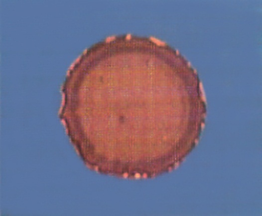
Figure 1a: Coating Failure from 11.77 J/cm2,
20ns Pulses @ 1064nm Wavelength Source due to Poor Process Control
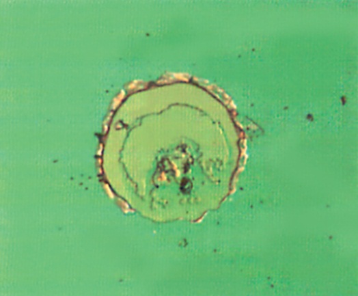
Figure 1b: Coating Failure from 12.92 J/cm2,
20ns Pulses @ 1064nm Wavelength Source due to Poor Process Control
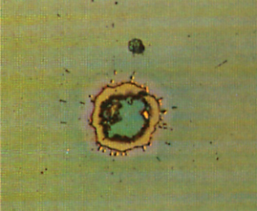
Figure 1c: Coating Failure from 14.3 J/cm2,
20ns Pulses @ 1064nm Wavelength Source due to Poor Process Control
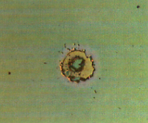
Figure 1d: Coating Failure from 73.3 J/cm2
Source due to Coating Defect
Fabrication of High-Power Optical Coatings
Substrate Preparation
Any organic or particulate residue from polishing or cleaning may absorb laser energy and is therefore a potential damage site. For this reason, the substrate and coating interface is a critical area in achieving high damage thresholds. Consequently, making high-power optical coatings requires tight control of every aspect of production, from initial substrate manufacturing to final packing. Before the optical element even reaches the coating chamber, its surface quality, subsurface quality, and cleanliness must be assured.
Substrates for use with high-power optical coatings must be high-quality. This is particularly important for refractive, or transmissive, optics - these substrates must demonstrate extremely low intrinsic absorption at the relevant wavelengths. To maximize transmission, it is important for the substrate to have as few surface quality defects as possible, as they can act as potential damage sites during irradiation. Surface quality is specified in terms of a scratch and dig value (the scratch number in units of .001mm, the dig number in units of .01mm). High-power laser optics typically call for less than 20-10 or 10-5 scratch-dig surface values.
The substrate must also be free of subsurface defects. This can be avoided through proper machining, grinding, and polishing methods prior to cleaning and coating. The first step is to begin with a blank large enough to allow for all necessary substrate removal. When machining, coating technicians carefully choose the appropriate tool feed, tool speed, and coolant flow in order to reduce subsurface stress and damage. Grinding is then done in incrementally smaller steps so as to achieve a more controlled surface. Finally, roughly 0.01 - 0.03mm is removed by polishing, which is used to remove subsurface damage caused by the previous steps.
Cleanliness
A clean coating chamber, appropriate choice of thin-film materials, and good control of process parameters are also essential. After deposition, coating technicians must carefully control contamination, which may lead to the formation of failure-inducing absorption sites. For this reason, meticulous cleaning procedures are also required at the assembly stage, typically under strict clean-room operating conditions.
This sensitivity to organic or particulate residue presents a very real challenge to coating technicians and underscores the importance of a thorough cleaning process. Clean-rooms are essential for minimizing the risk of recontamination after cleaning the optical element to be coated. Most manufacturers use lint-free wipes without silicone constituents when manually cleaning in their final clean process. Additionally, they use solvents of extremely high purity - typically, methanol, isopropanol, or acetone. Ultrasonic cleaning can be another useful tool as it is more effective (and less error-prone) at dislodging residual polishing compounds than cleaning by hand.
A typical multi-stage manual process includes a surfactant wash and several wipes with an ammonia solution followed by a drag-wipe technique. This drag-wipe stage produces very high shear forces, resulting in the removal of any remaining contaminants from the material’s surface.
Contaminants from the tools and walls of the coating chamber itself can also contribute to contamination of the substrate to be coated. For example, backstreaming can occur with an inefficient diffusion pump, resulting in organic contamination. Meanwhile, if excess material on the chamber walls is not removed prior to deposition, it can begin to flake off and loose particulates can be transferred onto the optical element. Preventing this is as easy as lining the walls with foil and periodically replacing it when it begins to exhibit excess material buildup.
Material Selection
Different materials are necessary when operating within certain wavelength ranges of the electromagnetic spectrum such as the ultraviolet (UV) or the visible/near-infrared (VIS-NIR) regions. Different materials are also used depending on whether or not the application calls for high-power continuous or high-power pulse irradiation. For example, continuous-wave (CW) lasers can cause an optical coating to heat up and melt, whereas short-pulse lasers can generate high-intensity electromagnetic fields.
Unfortunay, coating designers are limited by the number of materials suited for high-power applications. For example, high-reflective mirror coatings are created by alternating quarter-wavelength thick layers of high-index and low-index materials. The design of this stack of materials can significantly alter the laser-induced damage threshold (LIDT) of the coating. For instance, simply adding a half-wave thick layer of low-index material can drastically increase the LIDT. When choosing the appropriate low-index and high-index materials, coating technicians favor dielectric metal oxides because of their low absorptivity. Silicon dioxide (SiO2) is the generally accepted and ubiquitous choice for low-index layers; however, choosing a material for the high-index layers is not as straightforward: oxides of titanium, tantalum, zirconium, hafnium, scandium, and niobium are all popular choices.
Coating Design
LIDT values can be further increased by manipulating the coating layers in one of several ways. The electric-field distribution can be averaged across several layers, thereby avoiding a high electric-field concentration within a relatively small number of layers. Figures 2a – 2b show the normalized electric-field intensity (EFI) squared within a reflecting quarter-wave dielectric stack. The peak EFI values occur at layer interfaces and the highest EFIs occur at the layers closest to the air boundary. These EFI values can be reduced, however, by modifying the thicknesses of the four layers closest to air in a nine-layer stack. This has the effect of shifting the high-intensity resonant peaks from layer interfaces to locations within the film continuum. The highest-intensity resonant peaks can be positioned within the layers of the thin-film material demonstrating the highest damage threshold.
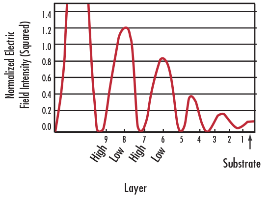
Figure 2a: Comparison of EFI to Layer within a Nine-Layer Stack Design
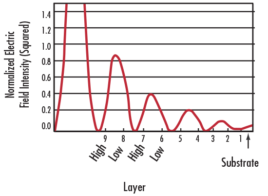
Figure 2b: Comparison of EFI to Layer within a Nine-Layer Stack Design with Layer Thicknesses Optimized to Decrease EFI
Coating Methods
As with standard optical coatings, there are three deposition methods available to coating technicians: thermal evaporation, ion-beam technology, and advanced plasma reactive sputtering (APRS). However, not all are suitable for high-power optical coatings.
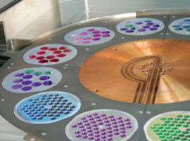
The thermal evaporation method is the most common method of producing high-power optical coatings in industry today, and Edmund Optics® is no exception. When enhanced with ion-assisted deposition (IAD), the thermal evaporation method (Figure 3) allows for more compact coatings with properties closer to those of the bulk materials. IAD also allows for greater control over layer thicknesses, which can decrease EFI values.
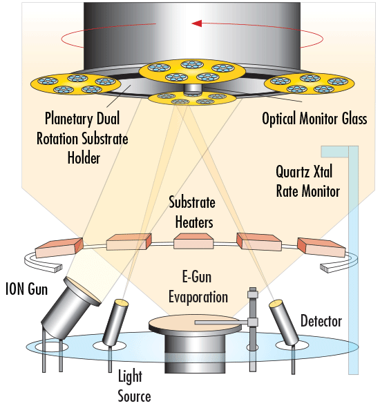
Figure 3: Evaporation Chamber with Ion-Assisted Deposition (IAD) Technology
Ion-beam technology is now a recognized and widely used tool in the manufacture of thin-film coatings, either as an enhancement to thermal evaporation (IAD) or as a sputtering technology (ion-beam sputtering (IBS)). IBS is an advanced deposition technique, but conclusive evidence does not exist to support it produces higher damage thresholds than the thermal evaporation method.
The advanced plasma reactive sputtering (APRS) technique is a state-of-the-art process, but is only used in applications with very tight specifications. For example, non-polarizing plate beamsplitters are candidates for APRS because of the low tolerances on S-polarized and P-polarized light separation. APRS is also rarely used with conventional optical elements because certain substrates which are best-suited for high-power applications cannot be sputtered with this method. In addition, evaporation usually has a greater capacity than APRS, meaning it can hold more substrates per coating run.
Coating Process Control
Many parameters play critical roles in the deposition of a high-power optical coating, including the rate of deposition, substrate temperature, oxygen partial pressure (used in designs including dielectric metal oxides), thickness calibration, material-melt preconditioning, and electron-gun sweep. A poorly controlled evaporation process produces spatter from the source, resulting in particulate condensates on the substrate surface and within the depositing coating. These condensates are potential damage defect sites. Unfortunay, some materials that can be used for high-damage-threshold coatings are difficult to deposit smoothly. The settings applied to the electron-gun sweep can be the difference between the production of a clear, high-damage-threshold coating and the production of a high-scatter coating with a much lower power capability.
The rate of deposition, substrate temperature, and oxygen partial pressure (for dielectric oxides) determine the stoichiometry of the growing film, which significantly affects the metal oxide chemistry in the depositing film. These parameters must be optimized and controlled to produce a homogeneous layer with the desired metal-oxygen content and structure.
In producing high-power anti-reflection (AR) coatings, thickness accuracy of the depositing films is an important factor in meeting the desired low reflectance. High-power high-reflective (mirror) coatings are generally less sensitive to small thickness errors as a result of relatively broad reflectance band afforded by the refractive index ratio of the high and low index layers. Deep-UV (DUV) mirror coatings are an exception, however, because material limitations in this spectral range produce relatively narrowband reflectors.
Testing High-Power Optical Coatings
Testing facilities offer a variety of tests that can determine the quality of a certain optical coating - from surface roughness and optical density to environmental exposure. For the purpose of this discussion, only the two methods of testing laser damage durability will be discussed: Damage Threshold Test and Durability Certification.
Damage Threshold Test (a.k.a. test until failure) - The optical coating is tested by irradiating the surface with a laser and increasing the output power until damage is observed. See Figures 1a - 1d for some real-world images of coating failures.
Durability Certification - The optical coating is tested according to a pre-determined specification or combination of specifications. Possible testing parameters include pulse rate, pulse duration, pulse count, irradiance, and/or beam diameter. The optical coating passes inspection only if it meets or exceeds the requirements set by the customer or manufacturer.
Coating Failure Factors
Coating technicians carefully monitor the effects of varying a number of testing parameters when testing high-power optical coatings. These same parameters are therefore important to optical designers when attempting to prevent laser damage. The following characteristics represent a few of the many parameters that can affect the laser-induced damage threshold (LIDT) of an optical coating:
Pulse Characteristics:
Duration - a measure of the length of an individual laser pulse (typically on the order of nanoseconds). This measurement is not as straightforward for non-rectangular pulses and is given as the full width of the pulse at half the maximum intensity (FWHM). LIDT values decrease exponentially as temporal pulse duration increases.
Shape - the temporal shape of the laser pulse (i.e. rectangular, triangular, Gaussian, etc.). Research has indicated that different shapes do have an impact on optical damage. For example, a rectangular pulse will result in coating damage at approximay 80% of the irradiance of a Gaussian beam with the same FWHM.
Beam Characteristics:
Mode of operation - transverse electromagnetic (TEM) wave patterns. LIDT values are much lower for multimode lasers as opposed to single mode lasers.
Wavelength - the wavelength of the laser source. LIDT values decrease as the wavelength decreases.
Intensity distribution - the distribution of energy intensity over the width of the beam (Gaussian is typical for most testing lasers as it is the most common in industry).
Angle of incidence - the angle at which the beam is deviated from the surface normal. LIDT values increase for increased values of angle of incidence due to increased reflection.
Spot size - the size of the beam on the surface of the coating. This measurement is taken using the full width of the beam at 1/e² intensity, where e is the maximum intensity value. LIDT values decrease as spot size decreases.
It is important for an optical designer to pay particular attention to the characteristics of optical coatings with respect to those of the intended source of irradiation. While not usually an issue with most low-power, commercial products, higher-powered lasers used in the optics, imaging, and photonics industries can lead to coating failure due to absorption sites or plasma burn. Optical designers and manufacturers can take steps to avoid such failures by carefully choosing an appropriate coating material, keeping a clean coating environment, and then testing the optical element for a given energy threshold specification.
版權所有 © 2025 江陰韻翔光電技術有限公司 備案號:蘇ICP備16003332號-1 技術支持:化工儀器網 管理登陸 GoogleSitemap


